M2F1G64CBH4B5(9)P / M2F2G64CB88B7(H)N / M2F4G64CB8HB5(9)N
1GB: 128M x 64 / 2GB: 256M x 64 / 4GB: 512M x 64
PC3-8500 / PC3-10600 / PC3-12800
Unbuffered DDR3 SDRAM DIMM
REV 1.1 22
© NANYA TECHNOLOGY CORPORATION
NANYA reserves the right to change products and specifications without notice.
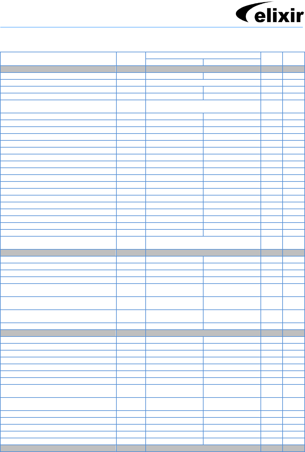
AC Timing Specifications for DDR3 SDRAM Devices Used on Module (1600MHz)
Minimum Clock Cycle Time (DLL off mode)
Refer to "Standard Speed Bins)
Min.: tCK(avg)min + tJIT(per)min
Max.: tCK(avg)max + tJIT(per)max
Absolute clock HIGH pulse width
Absolute clock LOW pulse width
Clock Period Jitter during DLL locking period
Cycle to Cycle Period Jitter
Cycle to Cycle Period Jitter during DLL locking period
Cumulative error across 2 cycles
Cumulative error across 3 cycles
Cumulative error across 4 cycles
Cumulative error across 5 cycles
Cumulative error across 6 cycles
Cumulative error across 7 cycles
Cumulative error across 8 cycles
Cumulative error across 9 cycles
Cumulative error across 10 cycles
Cumulative error across 11 cycles
Cumulative error across 12 cycles
Cumulative error across n = 13, 14 . . . 49, 50 cycles
tERR(nper)min = (1 + 0.68ln(n)) * tJIT(per)min
tERR(nper)max = (1 + 0.68ln(n)) * tJIT(per)max
DQS, DQS# to DQ skew, per group, per access
DQ output hold time from DQS, DQS#
DQ low-impedance time from CK, CK#
DQ high impedance time from CK, CK#
Data setup time to DQS, DQS# referenced to Vih(ac) / Vil(ac) levels
Data setup time to DQS, DQS# referenced to Vih(ac) / Vil(ac) levels
Data hold time from DQS, DQS# referenced to Vih(dc) / Vil(dc) levels
DQ and DM Input pulse width for each input
DQS,DQS# differential READ Preamble
DQS, DQS# differential READ Postamble
DQS, DQS# differential output high time
DQS, DQS# differential output low time
DQS, DQS# differential WRITE Preamble
DQS, DQS# differential WRITE Postamble
DQS, DQS# rising edge output access time from rising CK, CK#
DQS and DQS# low-impedance time
(Referenced from RL - 1)
DQS and DQS# high-impedance time
(Referenced from RL + BL/2)
DQS, DQS# differential input low pulse width
DQS, DQS# differential input high pulse width
DQS, DQS# rising edge to CK, CK# rising edge
DQS, DQS# falling edge setup time to CK, CK# rising edge
DQS, DQS# falling edge hold time from CK, CK# rising edge
Command and Address Timing
 (16 pages)
 Manymanuals.com
 Manymanuals.de
 Manymanuals.fr
 Manymanuals.it
 Manymanuals.pl
 Manymanuals.cz
 Manymanuals.es
 Manymanuals-pt.com
Comments to this Manuals